Design a 8 bit CISC simple and weird CPU
Hello there, in my last blog, I have designed my custom instruction set (ISA), LBK8. Now, I am going to design first CPU prototype that able to run the new ISA. In this blog, I will share my experience on designing this CPU and things need to be improved.
CPU architecture and details
To make thing simple, this CPU will be an uniprocessor CISC processor without pipeline. This will simplyify a lot of things but the code execution efficiency will be terrible. Then, this CPU will have 8 bit data bus and 8 bit address bus. However, both of them use the same line. For the cpu registers, there will be four general purpose registers due to address bit limit (only 2 bit). Meanwhile, ALU can perform 8 operation (addition, subtraction, shift left, shift right, and, not, or, compare).
Parts of CPU
Contol Unit (CU)
Since this is a CISC CPU, there will be two program counter, main counter and microcode counter. Main counter store the instruction pointer pointing to the current instruction in RAM. Meanwhile, the microcode counter execute the microcode with raw clock signal.
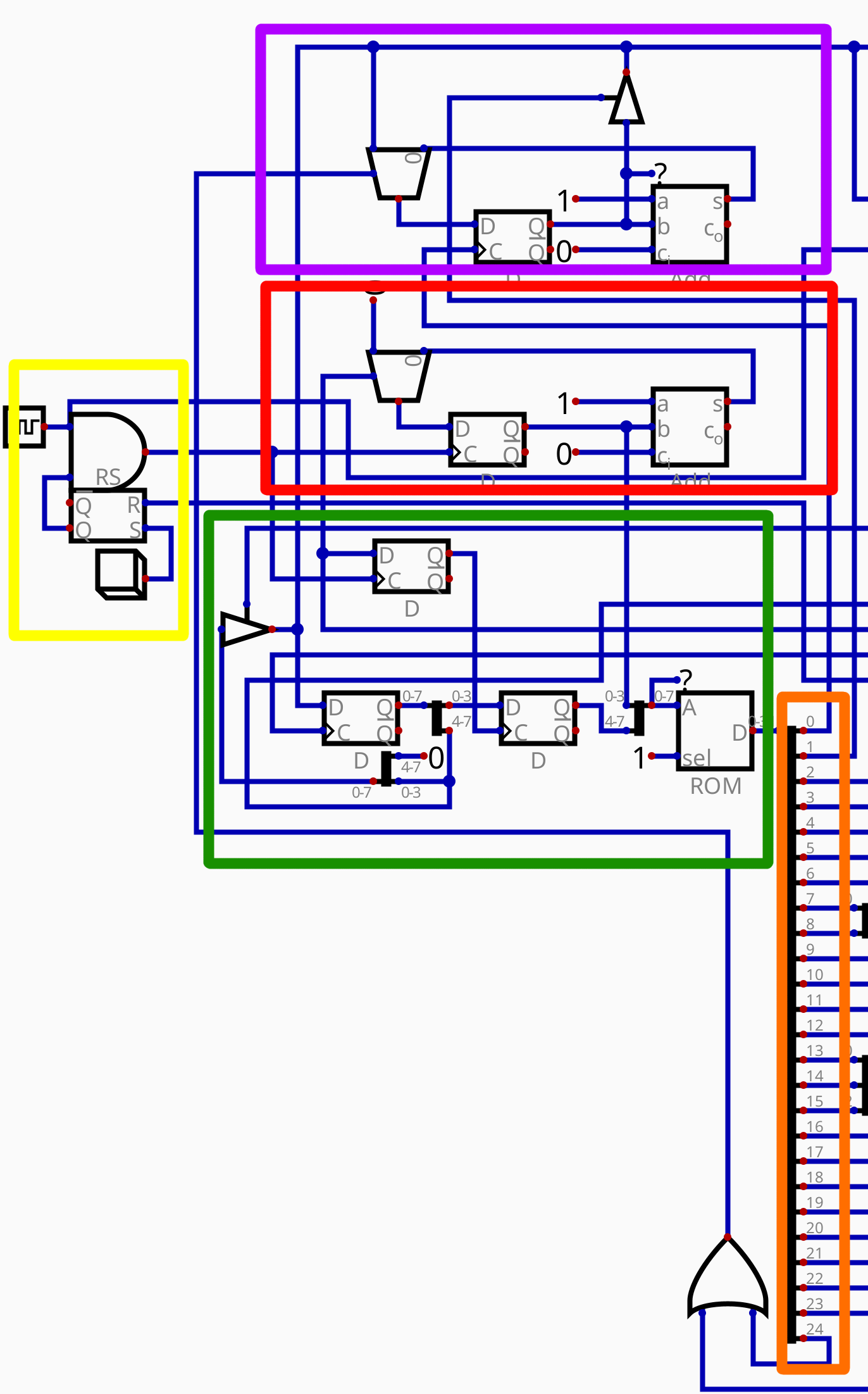
- Green - Microcode lookup table and executor
- Yellow - Clock controller
- Red - Microcode counter
- Purple - Main program counter
- Orange - 32 bit control bus
To perform microcode counter reset, it implement a two-stage register to clear microcode counter in two clock cycle.
Registers
There are four general purpose register in this CPU. However, only the first register, A is able to read and write data with RAM due to limitation of microcode and instruction. To show output, a 8bit hexidecimal seven segment display is connected to register D. The display can be controlled by writing desired value into register D.
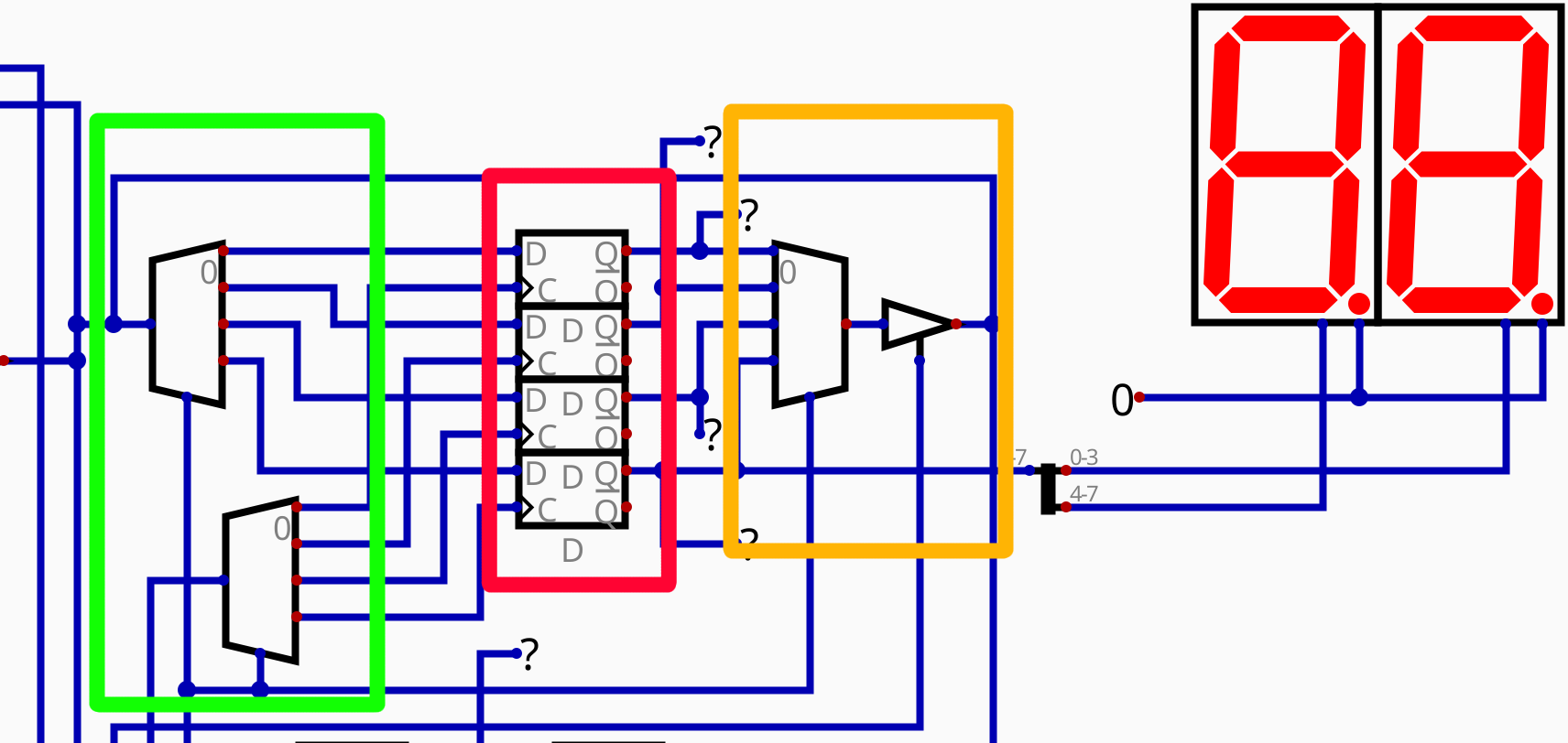
- Green - Multiplexer to control write of registers
- Red - Four registers.
- Orange - Demultiplexer to control read of registers
Arithmetic and Logic Unit (ALU)
This ALU is 8 bit and only able to do basic 8 operation.
- addition
- subtraction
- shift left
- shift right
- and
- not
- or
- compare
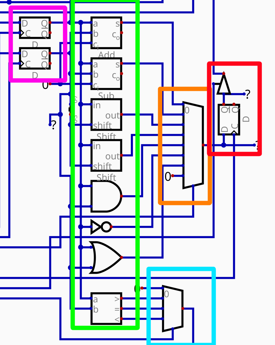
- Green - Operators
- Purple - Two input register to store parameter for operation
- Cyan - Comparation result selector
- Orange - ALU mode selector
- Red - ALU result register
Random access memory (RAM)
This RAM is 256 bytes size 8 bit wide RAM. Technically, this is an EEPROM instead of RAM because the program is stored in it before startup. Due to bad memory address map design, all the data is stored into a single chip.
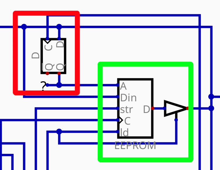
- Green - RAM chip
- Red - Memory address register (MAR)
Microcode design
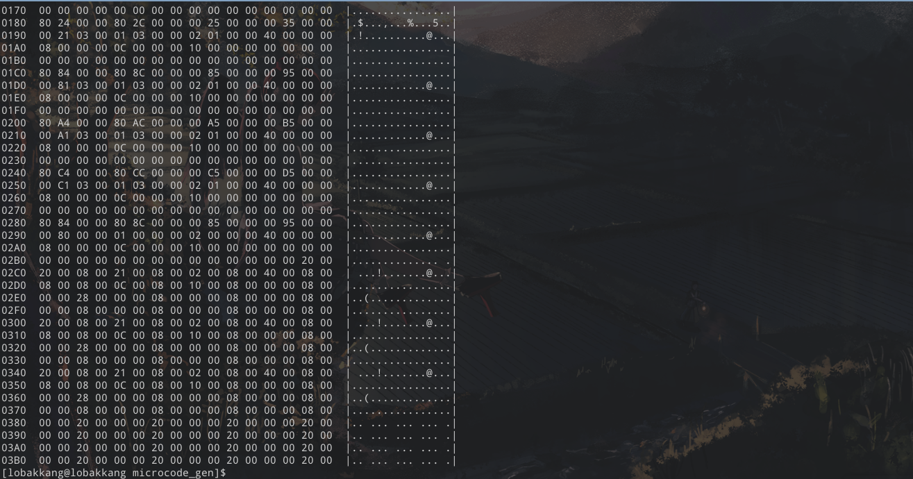
Although this is a very simple CPU, the microcode still can be quite complicated without using any tool. Unfortunately, I have no idea how to use industrial level EDA tool. So, I make my own tool instead. The microcode will be written in a spreadsheet using WPS.
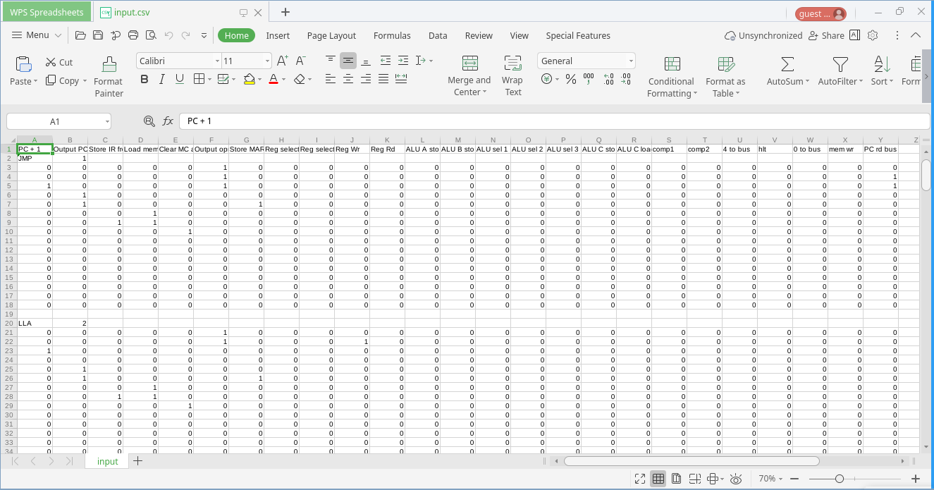
Then, the microcode will be exported as CSV file and convert into hex file using a python script. After that, the hex file will be loaded into the microcode lookup table which is made up of a ROM chip.
