Read and write Atmega328p "inwritable" internal flash
Recently, EEPROM in Atmega328p is not enough for me to store data during development of arang framework. It is only 1Kb meanwhile my aim is to store up to 20Kb of data in a small mCore. To meet my requirement, internal flash is a good choice but there is some limitations. For example, operation writing flash is painfully slow compared to EEPROM which is 3.3ms. Internal flash can only written 10,000 times meanwhile EEPROM write cycle is 100,000 times. Luckily, the frequency of the 20Kb data write is designed to be same as the frequency of bootloader writing sketch to flash.
How to write internal flash
Before that, we need to understand some mechanism inside Atmega328p. There are two section in internal flash, application section and bootloader section. The operation of writing internal flash can only be done in bootloader section. Now, the biggest problem for using internal flash is the code of arang framework is located in application section and has no access to write internal flash.
The first solution is just locate the code in bootloader section. Although this solution sounds easy, this can cause mCore unable to process stk500 commands from avrdude due to the default bootloader is replaced. Other than that, the configurable bootloader section is 2Kb and arang framework is far larger than 2Kb.
Then, I came up with another solution. Why not just jump to the small piece of code that can help us to write internal flash located at bootloader section whenever we want. After some research on Google, I found a open-source bootloader can achieve this. It is optiboot, a well-engineered bootloader that is only half Kb size.
Installing optiboot
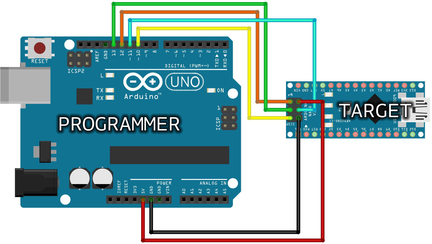
The method to flash a bootloader into Atmega328p is completely different from flashing a application section program. We have to use an external ISP instead of directly connect to PC. This is because during flashing bootloader, the default bootloader is overwritten and unable to run. To make a quick ISP, I upload a sketch called arduinoISP in arduino IDE example folder and connect it to mCore ICSP header using the following diagram that I get from Arduino Official website.

Preparing space for the data to be written
Writing data to internal flash need to be really careful because internal flash contain application section code, bootloader and some necessary data. To prevent the disaster of overwritten these data, we have to allocate an empty space for incoming data. To do it, I create a section in linker script right below arang framework. This section must be page align to prevent it is in same page with other section.
1 | |
You can get a full linker script at my Github repo :)
https://github.com/lobakkang/arang-framework/blob/main/linker.ld
Then, I fill the empty section with zero and a 69 (funny number) using some simple c syntax.
1 | |
The code is located at progmem.c line 9
https://github.com/lobakkang/arang-framework/blob/main/src/kernel/progmem.c
Call optiboot to write internal flash
To let arang framework “communicate” with optiboot, I copy an optiboot header file from its repo and include into the code. By using a function called optiboot_writePage from the header file to start the writing process. Here is an exaple code.
1 | |
Summary
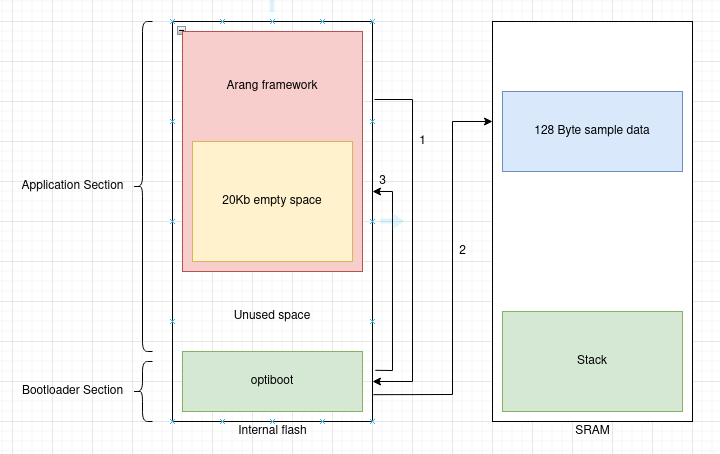
In the point of view of Atmega328p, the whole writing process will look like this:

- Arang framework call the function in optiboot
- optiboot read the sample data into a buffer page
- optiboot do all the magic and flash is written